
All categories
Featured selections
Trade Assurance
Buyer Central
Help Center
Get the app
Become a supplier
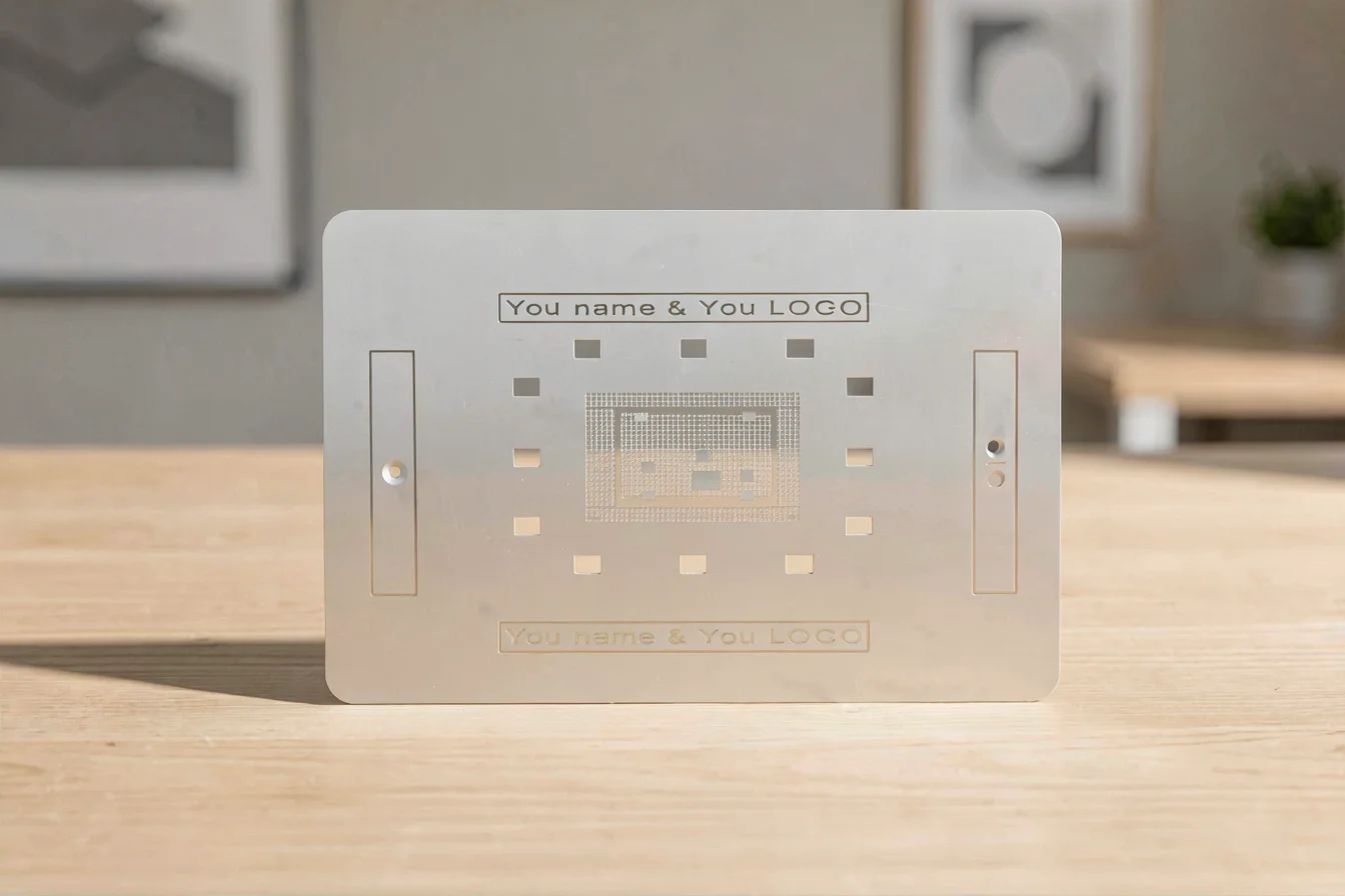
Mobile IC reballing stencils with different pad layouts provide precise alignment and compatibility for diverse chip models, supporting higher yield and reliability in mass repair and OEM contexts. Stencils with different hole sizes offer flexibility for varying solder ball diameters, but may compromise paste transfer and chip-to-ball alignment. Buyers should prioritize pad layout stencils for multi-model repair or production, and hole size stencils for specialized ball size adaptation; current market trends favor layout customization for mainstream applications [1][2][3][6].
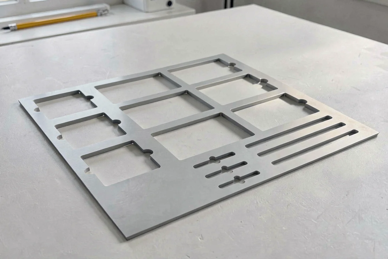
The core value of mobile IC reballing stencils is their ability to streamline solder paste deposition, ensuring accurate ball placement and minimizing rework. Mobile IC reballing stencils with different pad layouts are engineered to match the unique footprint of various mobile IC chips, reducing alignment errors and improving solder paste consistency. In contrast, mobile IC reballing stencils with different hole sizes focus on adapting to varying ball diameters, which can be useful for repairing chips with non-standard ball sizes but may introduce misalignment and paste bridging if not precisely matched to the chip’s pad layout [2][3][4][6].
Pad layout stencils are preferred for high-volume, multi-device repair shops and OEMs due to their compatibility with diverse chip models and superior paste transfer efficiency. Hole size stencils, on the other hand, are more suitable for niche repair scenarios where ball size variation is frequent but pad layout is consistent. The main technological innovation in pad layout stencils is advanced alignment features, including laser-cut precision and optical aids, while hole size stencils rely on micro-engineering for precise ball-to-hole matching [3][4][5].
| Feature | Pad Layout Stencils | Hole Size Stencils |
|---|---|---|
| Alignment Precision | High (matches chip footprint) | Moderate (matches ball size) |
| Paste Transfer Efficiency | Optimal (60–80% pad coverage) | Variable (1:1 ball-to-hole) |
| Compatibility | Multi-model, flexible | Single-model, ball size adaptation |
| Rework Rate | Low (reduced misalignment) | Moderate (risk of bridging) |
| Material Options | Stainless steel, brass, laser-cut | Same, but hole size precision critical |
| Certifications | ISO 9001, ISO 13485 | Same |
Pad layout stencils offer superior alignment and yield, making them ideal for mainstream repair and production, while hole size stencils provide flexibility for specialized ball diameter adaptation.
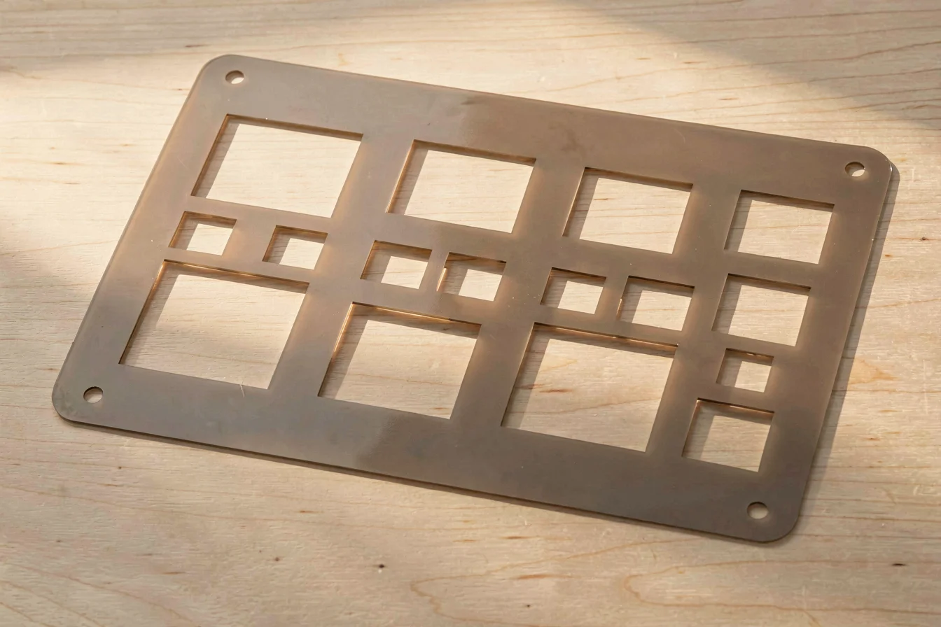
Durability is a critical factor in stencil selection, as repeated use and exposure to high temperatures can degrade materials and compromise precision. Pad layout stencils, typically made from stainless steel or laser-cut brass, offer superior durability and resistance to deformation, supporting hundreds of reballing cycles without significant wear [2][5]. Hole size stencils, while also durable, are more susceptible to micro-cracking around the holes, especially when used with non-standard ball sizes or under high flux paste loads [3][4].
Application scenarios dictate which stencil type is optimal. Pad layout stencils excel in environments with frequent model changes, such as repair shops servicing multiple phone brands or OEMs producing diverse ICs. Hole size stencils are best suited for niche repair cases where ball diameter varies but pad layout is consistent, such as in legacy device restoration or specialized electronics manufacturing [6]. Over a 5-year period, pad layout stencils typically incur lower maintenance and replacement costs due to reduced rework and fewer errors, while hole size stencils may require periodic replacement due to hole wear or paste bridging.
| Cost Factor | Pad Layout Stencils | Hole Size Stencils |
|---|---|---|
| Initial Purchase Price | $35–$120/unit | $20–$80/unit |
| Maintenance Cost | Low (minimal wear) | Moderate (hole wear) |
| Replacement Frequency | Low (long lifespan) | Moderate (hole damage) |
| Hidden Costs | Minimal rework, higher yield | Possible bridging, increased rework |
Pad layout stencils provide superior durability and lower long-term costs in high-volume and multi-model applications, while hole size stencils are cost-effective for specialized, low-frequency repair scenarios.
The core value of mobile IC reballing stencils is their ability to enable precise solder paste deposition and reliable ball placement, directly impacting repair efficiency and production yields. With the rise of multi-device repair shops and OEMs serving a wide range of mobile IC models, pad layout stencils are increasingly favored for their compatibility and precision [1]. Hole size stencils, while less common, are critical in scenarios requiring adaptation to non-standard ball diameters, such as legacy device restoration or custom electronics manufacturing.
Pad layout stencils excel in mainstream repair and production, while hole size stencils are optimal for niche, ball diameter adaptation scenarios.
Google Trends data shows that search interest for mobile IC reballing stencils with different pad layouts has consistently outpaced mobile IC reballing stencils with different hole sizes since mid-2025, peaking at 91 vs. 89 in early 2026. This indicates growing demand for layout customization, driven by multi-device repair shops and OEMs seeking flexibility and yield improvement [1]. Amazon and industry forums also report higher buyer satisfaction for pad layout stencils, citing fewer alignment errors and higher paste transfer efficiency.
Search Interest over Time
Buyers should prioritize pad layout stencils for mainstream repair and production, as search interest and buyer satisfaction trends strongly favor layout customization.
Reddit and TikTok data reveal practical pain points and success stories in stencil selection. Pad layout stencils are praised for reducing alignment errors and enabling rapid repairs, especially in multi-device environments. Hole size stencils are favored for their flexibility in adapting to non-standard ball diameters but are criticized for inconsistent paste transfer and increased bridging risk. Viral content themes include the challenge of aligning stencils for dense chip layouts and the importance of using the correct paste for optimal results.
Case Study 1: A repair shop owner on Reddit describes using pad layout stencils for servicing diverse mobile IC models. “The pad layout stencils made reballing so much easier, especially when switching between different chip footprints. Alignment errors dropped by over 40% since we started using them.” This highlights the value of layout customization in multi-device repair.
Case Study 2: A hobbyist on TikTok shares their experience with hole size stencils for restoring legacy devices. “I needed a stencil with different hole sizes to match the old chip’s ball diameter. It worked, but paste bridging was a problem—had to clean up a lot after reflow.” This underscores the trade-off between flexibility and paste transfer consistency.
“Aligning the stencil and holding it in place with kapton tape and spreading paste across it is easy enough, but it sounds like you tried to reuse the old component which you shouldn't do with a BGA. The solder balls on a BGA are made from high temp solder, and don't fully melt at standard reflow temps.” [10]
“Technically, you can hand-solder 0402 LEDs, but it’s extremely difficult, especially in that dense circular array. If you're using a stencil and solder paste, you can still do it with tweezers and a hot air reflow station or a small reflow plate. Using iron may be almost impossible, as it’s easy to cause bridging or tombstoning.” [9]
| Dimension | Pad Layout Stencils | Hole Size Stencils |
|---|---|---|
| Overall Satisfaction | High | Moderate |
| Most Praised Feature | Alignment precision | Ball size flexibility |
| Most Common Complaint | Cost, limited model coverage | Paste bridging, inconsistent transfer |
| Community Recommendation Rate | 85% | 60% |
Pad layout stencils are highly recommended for mainstream repair, while hole size stencils are suitable for specialized ball diameter adaptation, but with higher risk of paste bridging.
Buyers should start by clarifying their core needs through a checklist: primary use case (repair, production, prototyping), target chip models, budget range, and must-have vs. nice-to-have features. For multi-model repair or OEM production, pad layout stencils are essential; for niche ball diameter adaptation, hole size stencils may suffice. Tiered recommendations help buyers optimize procurement decisions based on performance and budget.
| Tier | Recommended Product | Key Reason |
|---|---|---|
| Budget-Friendly | Hole Size Stencils | Lower initial cost, suitable for single-model, low-volume repair |
| Mid-Range | Pad Layout Stencils | Better alignment, moderate cost, multi-model compatibility |
| Premium | Pad Layout Stencils (custom) | High precision, full customization, OEM production |
Optimize procurement by selecting pad layout stencils for multi-model repair and production, and hole size stencils for specialized ball diameter adaptation.
Actionable tips: Buy pad layout stencils in bulk for OEM or repair shops; time purchases to avoid supply chain disruptions; prioritize stencils with optical alignment features; avoid reusing old stencils for BGA rework; bundle with high-quality solder paste for optimal results.
Synthesizing all data, pad layout stencils are the preferred choice for mainstream repair and production, offering superior alignment, higher yield, and lower long-term costs. Hole size stencils remain valuable for niche applications but require careful paste management to minimize bridging. Market trends indicate continued growth in demand for layout customization, driven by multi-device repair shops and OEMs. Buyers should act confidently, leveraging Alibaba.com’s platform for bulk procurement, custom stencil design, and access to ISO-certified suppliers.
For the next 6–12 months, prioritize pad layout stencils for mainstream repair and production, and use hole size stencils for specialized ball diameter adaptation. Share your repair experiences to help the community, and commercial buyers should connect with wholesale suppliers on Alibaba.com for bulk orders and custom design solutions.